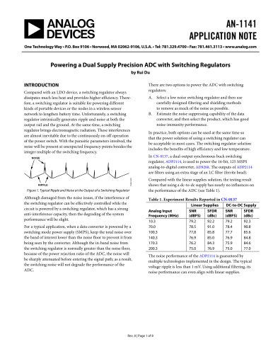
عضویت
عضویت  ورود اعضا
 راهنمای خرید


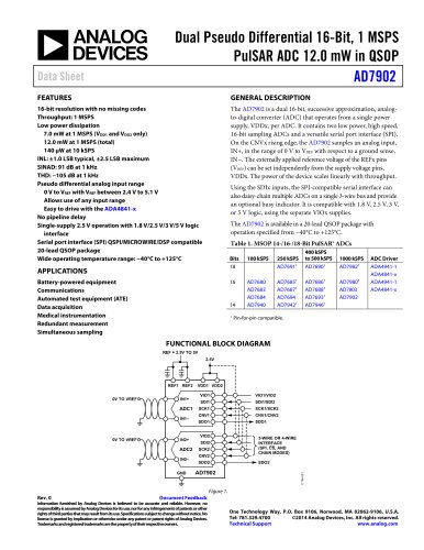
ADA49610 pages
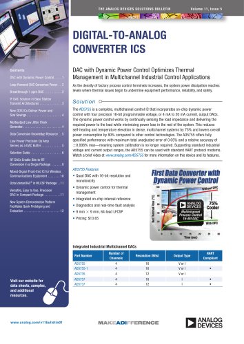
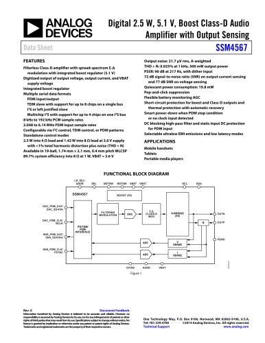
Low Distortion, 2.5 GHz, Differential DGA
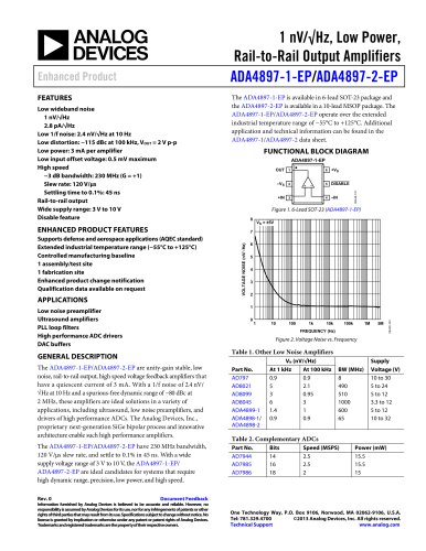
ADA4961
Preliminary Technical Data
FEATURES
High speed
−3 dB bandwidth: 2.5 GHz
−1 dB bandwidth: 1.8 GHz
Slew rate: 12 V/ns
Settling time to 0.1%: TBD ns
Overdrive recovery: TBD ns
Digitally adjustable gain
Voltage gain: −6 dB to +15 dB
Power gain: −3 dB to +18 dB
5-bit parallel or SPI bus gain control with fast attack
IMD3/HD3 distortion
IMD3 at 1 GHz: −90 dBc
HD3 at 500 MHz: −82 dBc
HD3 at 1 GHz: −80 dBc
HD3 at 1.5 GHz: −75 dBc
Low noise
Noise density RTO: 6.9 nV/√Hz
Noise figure: 5.6 dB at G = +15 dB
Differential impedances: 100 Ω input, 50 Ω output
Low power mode operation
Power-down control
Single 3.3 V or 5 V supply operation
Available in 24-lead, 4 mm × 4 mm LFSCP
APPLICATIONS
ADC driver for 12-bit to 14-bit Gs/s converters
RF/IF gain block
Line driver
Instrumentation
Satellite communications
Data acquisition
Military systems
GENERAL DESCRIPTION
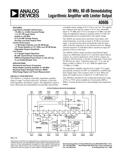
The ADA4961 is a high performance BiCMOS RF differential
amplifier (DGA) optimized for driving heavy loads out to 2.0
GHz and beyond. It typically achieves −90 dBc IMD3
performance at 500 MHz and −85 dBc at 1.5 GHz. The device
also exhibits very low output noise (6.8nv/√Hz). Together, these
performance numbers result in an SFDR of 133 dB/Hz at 1.5 GHz
and set a new benchmark for dynamic range for the power
consumed. This RF performance now allows GHz converters to
achieve their optimum performance with minimal limitations of
the driver amplifier or constraints on overall power that typically
result from GaAs amplifiers. This product can easily drive 10-bit
to 16-bit HS converters.
Rev. PrB
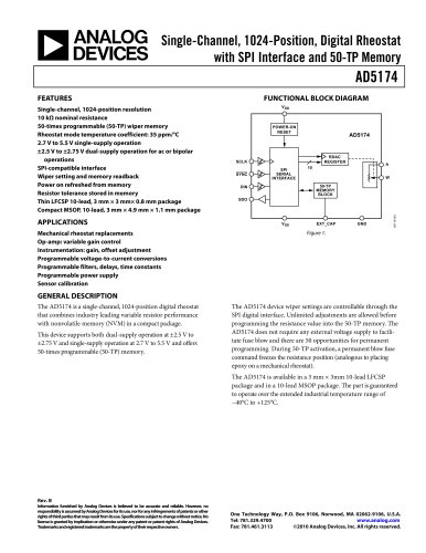
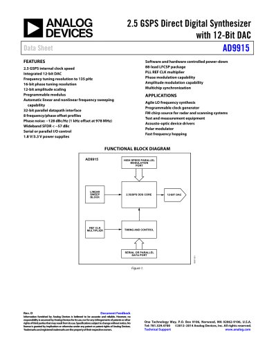
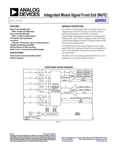
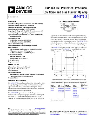
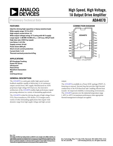
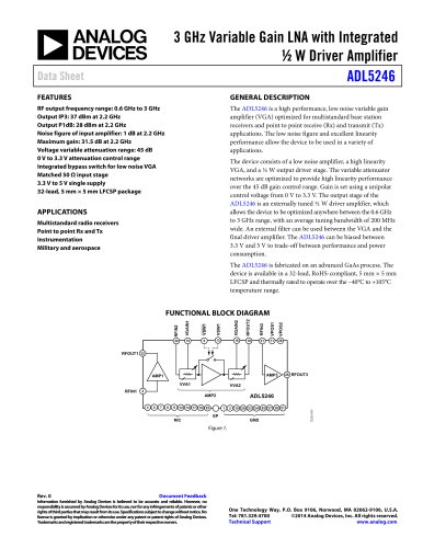
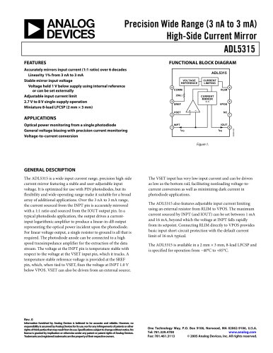
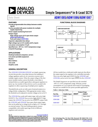
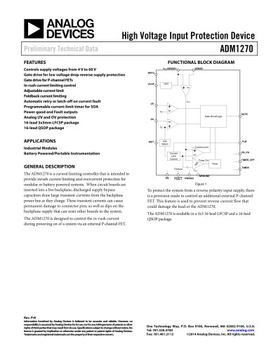
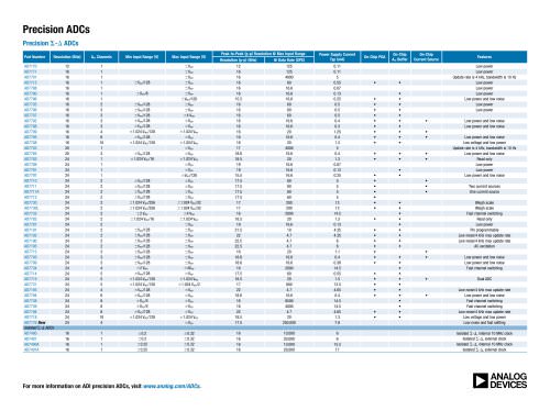
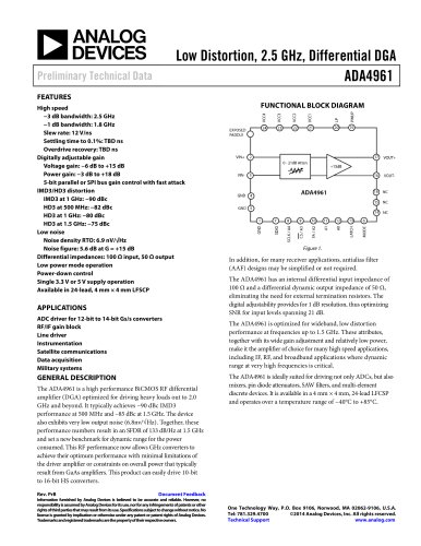
FUNCTIONAL BLOCK DIAGRAM
Figure 1.
In addition, for many receiver applications, antialias filter
(AAF) designs may be simplified or not required.
The ADA4961 has an internal differential input impedance of
100 Ω and a differential dynamic output impedance of 50 Ω,
eliminating the need for external termination resistors. The
digital adjustability provides for 1 dB resolution, thus optimizing
SNR for input levels spanning 21 dB.
The ADA4961 is optimized for wideband, low distortion
performance at frequencies up to 1.5 GHz. These attributes,
together with its wide gain adjustment and relatively low power,
make it the amplifier of choice for many high speed applications,
including IF, RF, and broadband applications where dynamic
range at very high frequencies is critical.
The ADA4961 is ideally suited for driving not only ADCs, but also
mixers, pin diode attenuators, SAW filters, and multi-element
discrete devices. It is available in a 4 mm × 4 mm, 24-lead LFCSP
and operates over a temperature range of −40°C to +85°C.
Document Feedback
Information furnished by Analog Devices is believed to be accurate and reliable. However, no
responsibility is assumed by Analog Devices for its use, nor for any infringements of patents or other
rights of third parties that may result from its use. Specifications subject to change without notice. No
license is granted by implication or otherwise under any patent or patent rights of Analog Devices.
Trademarks and registered trademarks are the property of their respective owners.
One Technology Way, P.O. Box 9106, Norwood, MA 02062-9106, U.S.A.
Tel: 781.329.4700
©2014 Analog Devices, Inc. All rights reserved.
Technical Support
www.analog.com