عضویت
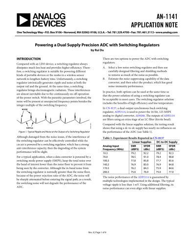
عضویت  ورود اعضا
 راهنمای خرید


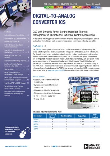
ADRF6720: Wideband Quadrature Modulator with Integrated Fractional-N PLL and VCOs0 pages
Wideband Quadrature Modulator with
Integrated Fractional-N PLL and VCOs
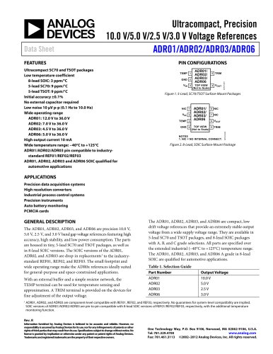
ADRF6720
Data Sheet
FEATURES
GENERAL DESCRIPTION
I/Q modulator with integrated fractional-N PLL
RF output frequency range: 700 MHz to 3000 MHz
Internal LO frequency range: 356.25 MHz to 2855 MHz
Output P1dB: 12.2 dBm at 2140 MHz
Output IP3: 32.6 dBm at 2140 MHz
Carrier feedthrough: −40.3 dBm at 2140 MHz
Sideband suppression: −37.6 dBc at 2140 MHz
Noise floor: −157.9 dBm/Hz at 2140 MHz
Baseband 1 dB modulation bandwidth: >1000 MHz
Baseband input bias level: 0.5 V
Power supply: 3.3 V/425 mA
Integrated RF tunable balun allowing single-ended RF output
Multicore integrated VCOs
HD3/IP3 optimization
Sideband suppression and carrier feedthrough optimization
High-side/low-side LO injection
Programmable via 3-wire serial port interface (SPI)
40-lead 6 mm × 6 mm LFCSP
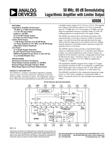
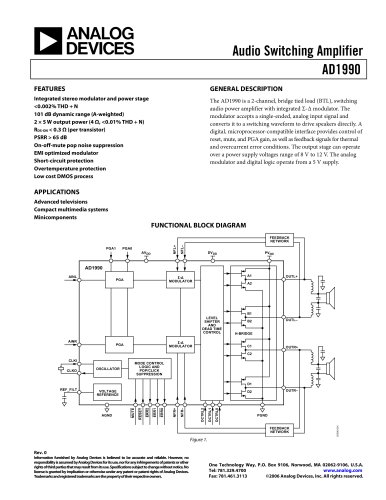
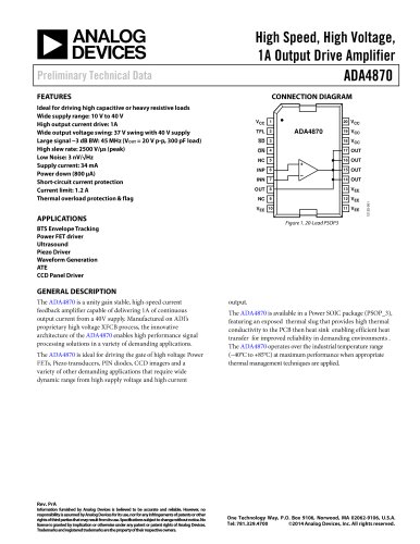
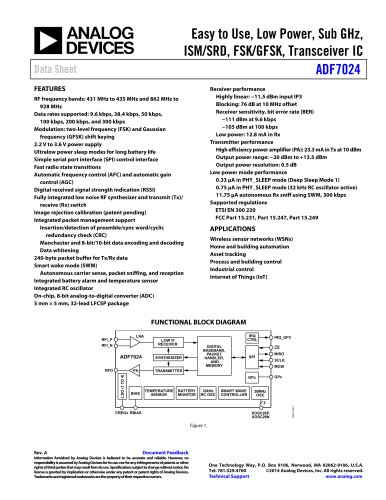
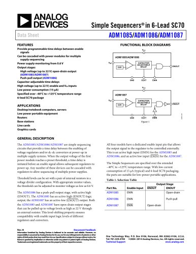
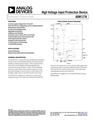
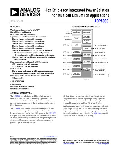
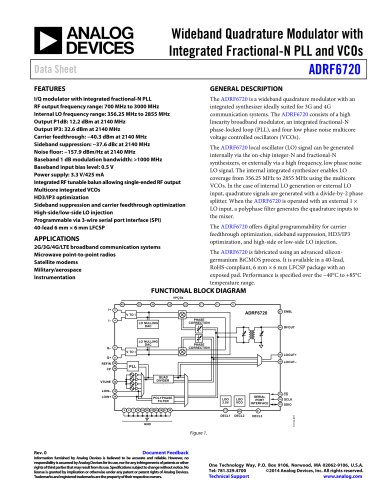
The ADRF6720 is a wideband quadrature modulator with an
integrated synthesizer ideally suited for 3G and 4G
communication systems. The ADRF6720 consists of a high
linearity broadband modulator, an integrated fractional-N
phase-locked loop (PLL), and four low phase noise multicore
voltage controlled oscillators (VCOs).
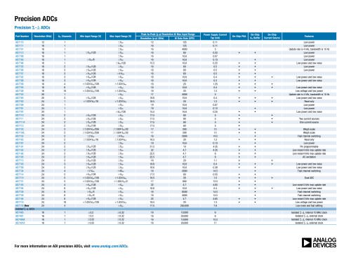
The ADRF6720 local oscillator (LO) signal can be generated
internally via the on-chip integer-N and fractional-N
synthesizers, or externally via a high frequency, low phase noise
LO signal. The internal integrated synthesizer enables LO
coverage from 356.25 MHz to 2855 MHz using the multicore
VCOs. In the case of internal LO generation or external LO
input, quadrature signals are generated with a divide-by-2 phase
splitter. When the ADRF6720 is operated with an external 1 ×
LO input, a polyphase filter generates the quadrature inputs to
the mixer.
The ADRF6720 offers digital programmability for carrier
feedthrough optimization, sideband suppression, HD3/IP3
optimization, and high-side or low-side LO injection.
APPLICATIONS
2G/3G/4G/LTE broadband communication systems
Microwave point-to-point radios
Satellite modems
Military/aerospace
Instrumentation
The ADRF6720 is fabricated using an advanced silicongermanium BiCMOS process. It is available in a 40-lead,
RoHS-compliant, 6 mm × 6 mm LFCSP package with an
exposed pad. Performance is specified over the −40°C to +85°C
temperature range.
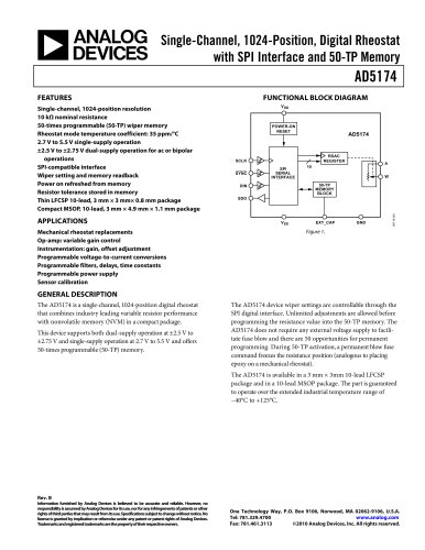
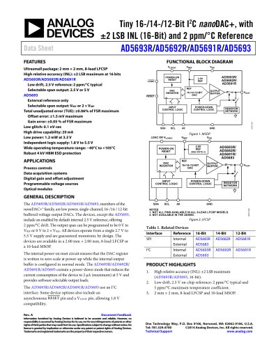
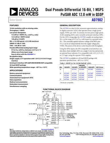
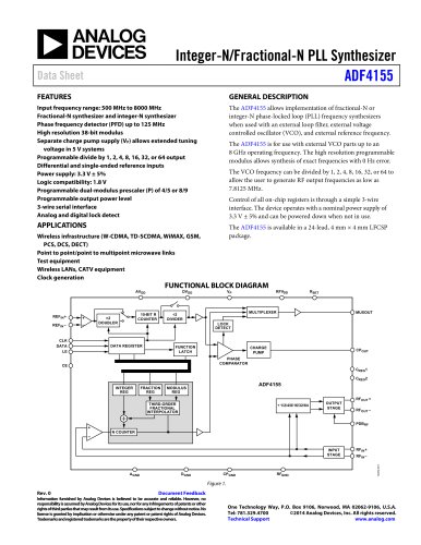
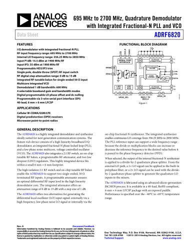
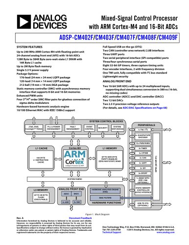
FUNCTIONAL BLOCK DIAGRAM
VPOSx
40
I+
35
30
26
22
17
11
6
3
LO NULLING
DAC
Q–
8
LOOUT+
LOOUT–
15
LO NULLING
DAC
RFOUT
19
4
ENBL
18
I–
27
24
ADRF6720
V TO I
CS
14
SCLK
13
SDIO
PHASE
CORRECTION
PHASE
CORRECTION
V TO I
9
REFIN
39
CP
36
VTUNE
32
LOIN–
33
LOIN+
34
PLL
QUAD
DIVIDER
POLYPHASE
FILTER
5
12
7 10 16 20 23 25 29 37 38
LDO
VCO
28
DECL1
2
LDO
2.5V
DECL2
GND
SERIAL
PORT
INTERFACE
31
DECL3
12134-001
Q+
Figure 1.
Rev. 0
Document Feedback
Information furnished by Analog Devices is believed to be accurate and reliable. However, no
responsibility is assumed by Analog Devices for its use, nor for any infringements of patents or other
rights of third parties that may result from its use. Specifications subject to change without notice. No
license is granted by implication or otherwise under any patent or patent rights of Analog Devices.
Trademarks and registered trademarks are the property of their respective owners.
One Technology Way, P.O. Box 9106, Norwood, MA 02062-9106, U.S.A.
Tel: 781.329.4700
©2014 Analog Devices, Inc. All rights reserved.
Technical Support
www.analog.com
"