عضویت
عضویت  ورود اعضا
 راهنمای خرید


ADN2915: Continuous Rate 6.5 Mbps to 11.3 Gbps Clock and Data Recovery IC with Integrated Limiting Amp/EQ0 pages
Continuous Rate 6.5 Mbps to 11.3 Gbps Clock and
Data Recovery IC with Integrated Limiting Amp/EQ
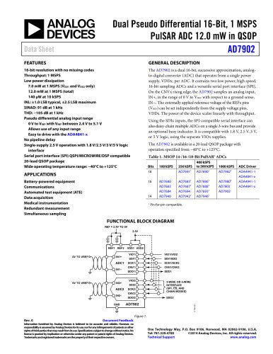
ADN2915
Data Sheet
FEATURES
GENERAL DESCRIPTION
Serial data input: 6.5 Mbps to 11.3 Gbps
No reference clock required
Exceeds SONET/SDH requirements for jitter
transfer/generation/tolerance
Quantizer sensitivity: 7.3 mV typical (limiting amplifier mode)
Optional limiting amplifier, equalizer, and bypass inputs
Programmable jitter transfer bandwidth to support G.8251 OTN
Programmable slice level
Sample phase adjust (5.65 Gbps or greater)
Output polarity invert
Programmable LOS threshold via I2C
I2C to access optional features
Loss of signal (LOS) alarm (limiting amplifier mode only)
Loss of lock (LOL) indicator
PRBS generator/detector
Application-aware power
430 mW at 11.3 Gbps, equalizer enabled, no clock output
380 mW at 6.144 Gbps, limiting amplifier mode, no clock
output
340 mW at 622 Mbps, input bypass mode, no clock output
Power supply: 1.2 V, flexible 1.8 V to 3.3 V, and 3.3 V
4 mm × 4 mm 24-lead LFCSP
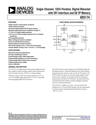
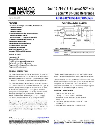
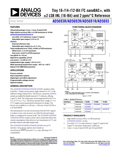
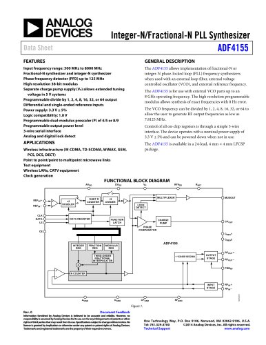
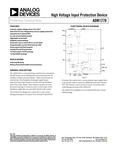
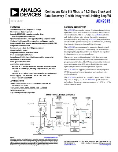
The ADN2915 provides the receiver functions of quantization,
signal level detect, and clock and data recovery for continuous
data rates from 6.5 Mbps to 11.3 Gbps. The ADN2915 automatically locks to all data rates without the need for an external
reference clock or programming. ADN2915 jitter performance
exceeds all jitter specifications required by SONET/SDH, including
jitter transfer, jitter generation, and jitter tolerance.
The ADN2915 provides manual or automatic slice adjust and
manual sample phase adjusts. Additionally, the user can select a
limiting amplifier, equalizer, or bypass at the input. The equalizer
is either adaptive or can be manually set.
The receiver front-end loss of signal (LOS) detector circuit
indicates when the input signal level has fallen below a userprogrammable threshold. The LOS detect circuit has hysteresis
to prevent chatter at the LOS output. In addition, the input
signal strength can be read through the I2C registers.
The ADN2915 also supports pseudorandom binary sequence
(PRBS) generation, bit error detection, and input data rate
readback features.
The ADN2915 is available in a compact 4 mm × 4 mm, 24-lead
chip scale package (LFCSP). All ADN2915 specifications are
defined over the ambient temperature range of −40°C to +85°C,
unless otherwise noted.
APPLICATIONS
SONET/SDH OC-1/OC-3/OC-12/OC-48/OC-192 and all
associated FEC rates
1GFC, 2GFC, 4GFC, 8GFC, 10GFC, 1GE, and 10GE
WDM transponders
Any rate regenerators/repeaters
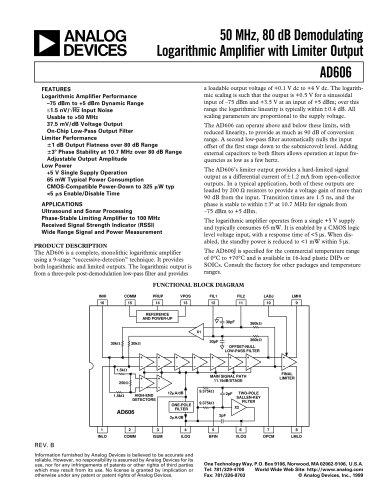
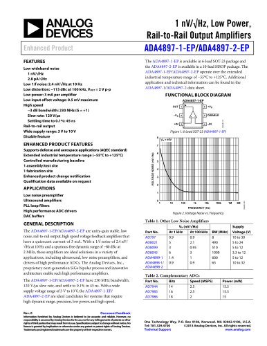
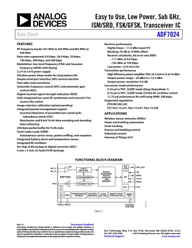
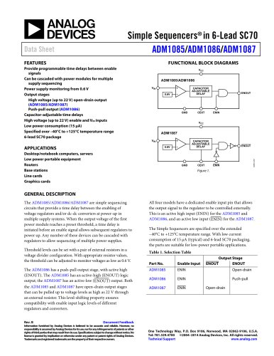
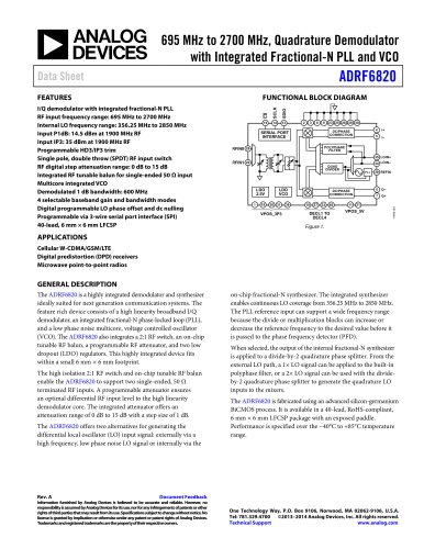
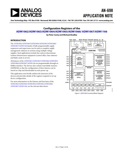
FUNCTIONAL BLOCK DIAGRAM
SCK
SDA
LOL
I2C REGISTERS
FREQUENCY
ACQUISITION
AND LOCK
DETECTOR
LOS
THRESH
SLICE
ADJUST
I2C_ADDR
REFCLKP/
REFCLKN
(OPTIONAL)
DATOUTP/
DATOUTN
CML
CLK
DDR
LOS
DETECT
TXD
FIFO
SAMPLE
PHASE
ADJUST
÷N
DOWNSAMPLER
AND LOOP
FILTER
LA
PIN
DATA
INPUT
SAMPLER
2
BYPASS
NIN
50Ω
50Ω
I2C
VCM
CML
DATA RATE
ADN2915
LOS
CLKOUTP/
CLKOUTN
÷2
DCO
RXD
RXCK
EQ
CLOCK
I2C
PHASE
SHIFTER
08413-001
VCC
FLOAT
Figure 1.
Rev. 0
Document Feedback
Information furnished by Analog Devices is believed to be accurate and reliable. However, no
responsibility is assumed by Analog Devices for its use, nor for any infringements of patents or other
rights of third parties that may result from its use. Specifications subject to change without notice. No
license is granted by implication or otherwise under any patent or patent rights of Analog Devices.
Trademarks and registered trademarks are the property of their respective owners.
One Technology Way, P.O. Box 9106, Norwood, MA 02062-9106, U.S.A.
Tel: 781.329.4700
©2013 Analog Devices, Inc. All rights reserved.
Technical Support
www.analog.com