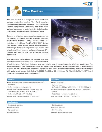
عضویت
عضویت  ورود اعضا
 راهنمای خرید


ESD Protection for USB3.00 pages

A P P L I C AT I O N N OT E
ESD Protection for USB 3.0 (SuperSpeed USB) Ports
Protection Technology Developments
The rapid increase in the bandwidth to the connectors
created another protection challenge; the chipset’s interface
speeds increased and silicon feature sizes decreased. This
combination of faster speed and smaller I/O cells led to
increased ESD susceptibility for the chipset’s PHY I/O’s, while
limiting the external impedance loading budget to the point
where low-cap ESD was no longer low enough.
As a result, designers have transitioned from copying-and-
Overview
1. Universal Serial Bus (USB) Protection History
In 1999 when it was introduced, the USB 2.0 interface’s
480Mbps half-duplex differential channel presented a difficult
challenge for designers implementing electrostatic discharge
(ESD) protection when the range of low-capacitance, or “lowcap,” Transient Voltage Suppressors (TVSs) comprised 1-1.2pF
discrete diodes. The subsequent USB 3.0, or SuperSpeed
USB, interface maintains the exact physical 2.0 interface, and
complicates the protection problem by adding two 5Gbps
half-duplex differential pairs (one Tx and one Rx pair), as
shown in Figure 1.
Discrete TVS markets in the past lagged behind Moore’s Law.
While CPU clock speeds and memory sizes scaled internally,
the external I/O interfaces of digital devices followed at a
slower rate. As internal IC parallel PCI busses were upgraded
to internal serial links (PCI Express), external I/O consolidated
pasting generic discrete ESD component layouts into new
designs, to performing careful board characterization with
respect to timing, matched impedances and insertion loss.
ESD Protection for USB 3.0
When adding ESD protection to USB 3.0 systems it is
essential to consider the potential impact of additional
capacitance and inductance on the timing of the chosen
device on the high-speed differential pairs. When operating
at 5Gbps on each of the SuperSpeed USB differential pairs,
any additional impedance on the line can distort the signal,
leading to:
•t
diagrams for rise times and signal levels,
•t
additional constraints on board design,
•t
lower system level performance, and
•t
interoperability issues with different cables (quality
and length).
down into high-speed differential links such as USB, FireWire,
and eSATA interfaces.
greater difficulty in meeting the required eye
To minimize timing impact on these high-speed lines, and to
provide adequate protection to the downstream chipset, there
are four, key technical considerations to be made regarding
the ESD protection device:
1.t
Low capacitance / low insertion loss for optimal
signal integrity
2.t
ESD device robustness and interaction with the
downstream protected IC
3.t
A small, flow-through ESD device package
4.t
An optimized layout
Figure 1. USB 3.0 adds two 5Gbps half differential pairs compared to USB 2.0.
1
www.circuitprotection.com
© 2011 Tyco Electronics Corporation. All Rights Reserved. | TE Connectivity, TE connectivity (logo) and TE (logo) are trademarks. Other products, logos and company names mentioned herein may be trademarks of their respective owners.
"