عضویت
عضویت  ورود اعضا
 راهنمای خرید


ACS7110 pages

ACS711
Hall Effect Linear Current Sensor with Overcurrent
Fault Output for <100 V Isolation Applications
Features and Benefits
Description
▪ No external sense resistor required; single package solution
▪ Reduced Power Loss:
The Allegro™ ACS711 provides economical and precise
solutions for AC or DC current sensing in <100 V audio,
communications systems, and white goods. The device package
allows for easy implementation by the customer. Typical
applications include circuit protection, current monitoring,
and motor and inverter control.
▫ 0.6 mΩ internal conductor resistance on EX package
▫ 1.2 mΩ internal conductor resistance on LC package
▪
▪
▪
▪
▪
▪
▪
▪
▪
▪
▪
▪
▪
▪
Economical low- and high-side current sensing
Output voltage proportional to AC or DC currents
±12.5 A and ±25 A full scale sensing ranges on LC package
±15.5 A and ±31 A full scale sensing ranges on EX package
¯ ¯¯¯
Overcurrent ¯ ¯ ¯ ¯ ¯ trips and latches at 100% of full-scale current
FAULT
Low-noise analog signal path
100 kHz bandwidth
Small footprint, low-profile SOIC8 and QFN packages
3.0 to 5.5 V, single supply operation
Integrated electrostatic shield for output stability
Factory-trimmed for accuracy
Extremely stable output offset voltage
Zero magnetic hysteresis
Ratiometric output from supply voltage
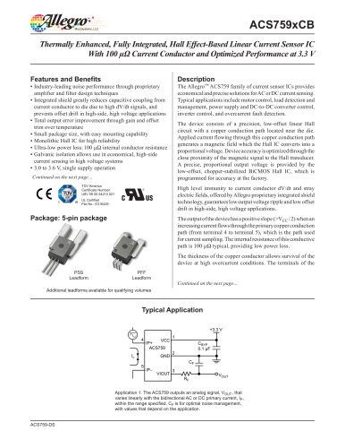
Packages:
8-pin SOICN
with internally fused path
(LC package)
The device consists of a linear Hall sensor circuit with a copper
conduction path located near the surface of the die. Applied
current flowing through this copper conduction path generates
a magnetic field which is sensed by the integrated Hall IC
and converted into a proportional voltage. Device accuracy is
optimized through the close proximity of the magnetic signal
to the Hall transducer.
The output of the device has a positive slope proportional to
the current flow from IP+ to IP– (pins 1 and 2, to pins 3 and
4). The internal resistance of this conductive path is 0.6 mΩ
for the EX package, and 1.2 mΩ for the LC package, providing
a non-intrusive measurement interface that saves power in
applications that require energy efficiency.
The ACS711 is optimized for low-side current sensing
applications, although the terminals of the conductive path
are electrically isolated from the sensor IC leads, providing
sufficient internal creepage and clearance dimensions for a
low AC or DC working voltage applications. The thickness
12-contact QFN
3 mm × 3 mm × 0.75 mm
(EX package)
Continued on the next page…
Approximate Scale 1:1
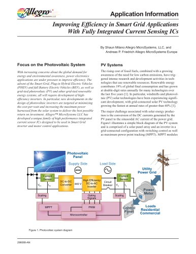
Typical Application
+3.3 V
IP+
VCC
CBYP
0.1 μF
IP+
VIOUT
IP
ACS711
IP–
IP–
RPU
CLOAD
FAULT
GND
Application 1. The ACS711 outputs an analog signal, VIOUT , that varies linearly with the
¯ L¯
¯
bi-directional AC or DC primary current, IP , within the range specified. The ¯ ¯¯¯ ¯ pin trips
FAU¯ T
when IP reaches ±100% of its full-scale current.
ACS711A-DS, Rev. 2