عضویت
عضویت  ورود اعضا
 راهنمای خرید


ACS7590 pages
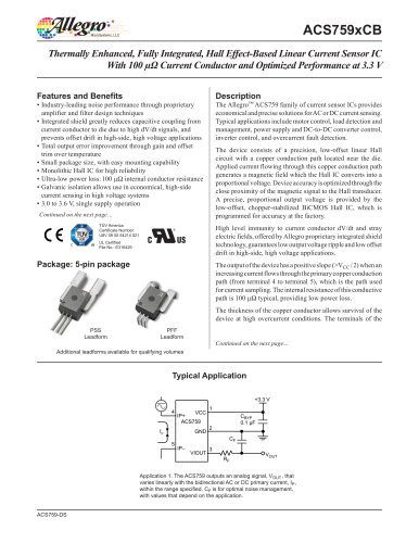
ACS759xCB
Thermally Enhanced, Fully Integrated, Hall Effect-Based Linear Current Sensor IC
With 100 μΩ Current Conductor and Optimized Performance at 3.3 V
Features and Benefits
Description
▪ Industry-leading noise performance through proprietary
amplifier and filter design techniques
▪ Integrated shield greatly reduces capacitive coupling from
current conductor to die due to high dV/dt signals, and
prevents offset drift in high-side, high voltage applications
▪ Total output error improvement through gain and offset
trim over temperature
▪ Small package size, with easy mounting capability
▪ Monolithic Hall IC for high reliability
▪ Ultra-low power loss: 100 μΩ internal conductor resistance
▪ Galvanic isolation allows use in economical, high-side
current sensing in high voltage systems
▪ 3.0 to 3.6 V, single supply operation
The Allegro™ ACS759 family of current sensor ICs provides
economical and precise solutions for AC or DC current sensing.
Typical applications include motor control, load detection and
management, power supply and DC-to-DC converter control,
inverter control, and overcurrent fault detection.
The device consists of a precision, low-offset linear Hall
circuit with a copper conduction path located near the die.
Applied current flowing through this copper conduction path
generates a magnetic field which the Hall IC converts into a
proportional voltage. Device accuracy is optimized through the
close proximity of the magnetic signal to the Hall transducer.
A precise, proportional output voltage is provided by the
low-offset, chopper-stabilized BiCMOS Hall IC, which is
programmed for accuracy at the factory.
Continued on the next page…
pe d
Ty ste
te
TÜV America
Certificate Number:
U8V 09 05 54214 021
High level immunity to current conductor dV/dt and stray
electric fields, offered by Allegro proprietary integrated shield
technology, guarantees low output voltage ripple and low offset
drift in high-side, high voltage applications.
UL Certified
File No.: E316429
Package: 5-pin package
The output of the device has a positive slope (>VCC / 2) when an
increasing current flows through the primary copper conduction
path (from terminal 4 to terminal 5), which is the path used
for current sampling. The internal resistance of this conductive
path is 100 μΩ typical, providing low power loss.
The thickness of the copper conductor allows survival of the
device at high overcurrent conditions. The terminals of the
PSS
Leadform
PFF
Leadform
Continued on the next page…
Additional leadforms available for qualifying volumes
Typical Application
+3.3 V
4
VCC
IP+
ACS759
IP
GND
5
1
CBYP
0.1 μF
2
CF
IP–
VIOUT
3
RF
VOUT
Application 1. The ACS759 outputs an analog signal, VOUT , that
varies linearly with the bidirectional AC or DC primary current, IP ,
within the range specified. CF is for optimal noise management,
with values that depend on the application.
ACS759-DS