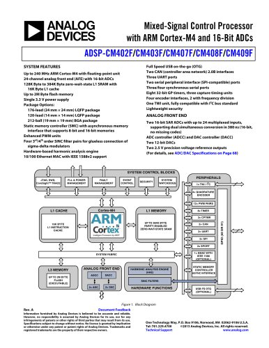
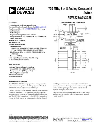
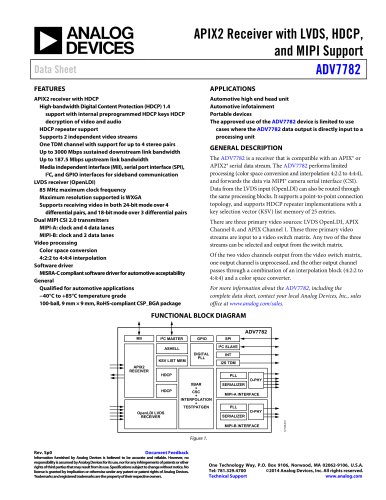
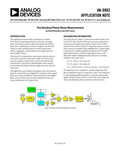
عضویت
عضویت  ورود اعضا
 راهنمای خرید


ADL52460 pages
3 GHz Variable Gain LNA with Integrated
½ W Driver Amplifier
ADL5246
Data Sheet
FEATURES
GENERAL DESCRIPTION
RF output frequency range: 0.6 GHz to 3 GHz
Output IP3: 37 dBm at 2.2 GHz
Output P1dB: 28 dBm at 2.2 GHz
Noise figure of input amplifier: 1 dB at 2.2 GHz
Maximum gain: 31.5 dB at 2.2 GHz
Voltage variable attenuation range: 45 dB
0 V to 3.3 V attenuation control range
Integrated bypass switch for low noise VGA
Matched 50 Ω input stage
3.3 V to 5 V single supply
32-lead, 5 mm × 5 mm LFCSP package
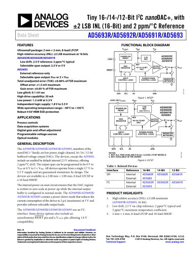
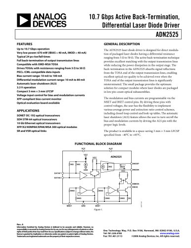
The ADL5246 is a high performance, low noise variable gain
amplifier (VGA) optimized for multistandard base station
receivers and point to point receive (Rx) and transmit (Tx)
applications. The low noise figure and excellent linearity
performance allow the device to be used in a variety of
applications.
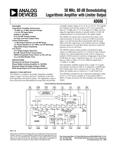
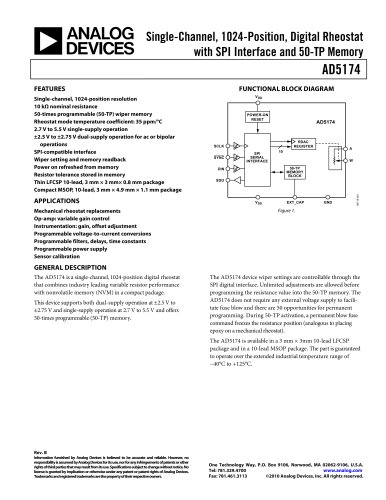
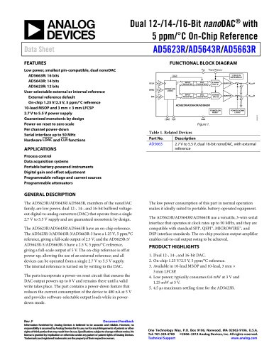
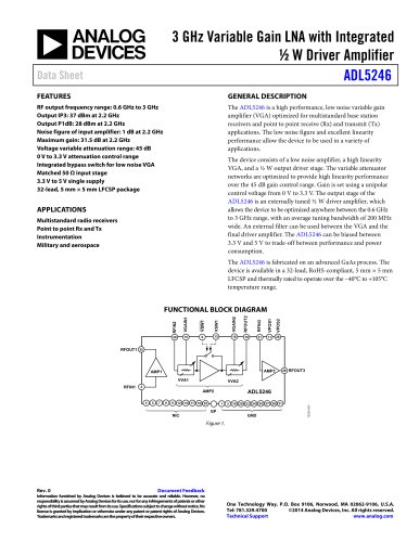
The device consists of a low noise amplifier, a high linearity
VGA, and a ½ W output driver stage. The variable attenuator
networks are optimized to provide high linearity performance
over the 45 dB gain control range. Gain is set using a unipolar
control voltage from 0 V to 3.3 V. The output stage of the
ADL5246 is an externally tuned ½ W driver amplifier, which
allows the device to be optimized anywhere between the 0.6 GHz
to 3 GHz range, with an average tuning bandwidth of 200 MHz
wide. An external filter can be used between the VGA and the
final driver amplifier. The ADL5246 can be biased between
3.3 V and 5 V to trade-off between performance and power
consumption.
APPLICATIONS
Multistandard radio receivers
Point to point Rx and Tx
Instrumentation
Military and aerospace
The ADL5246 is fabricated on an advanced GaAs process. The
device is available in a 32-lead, RoHS-compliant, 5 mm × 5 mm
LFCSP and thermally rated to operate over the −40°C to +105°C
temperature range.
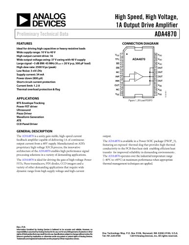
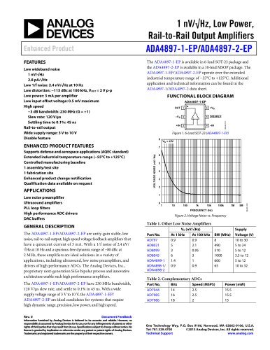
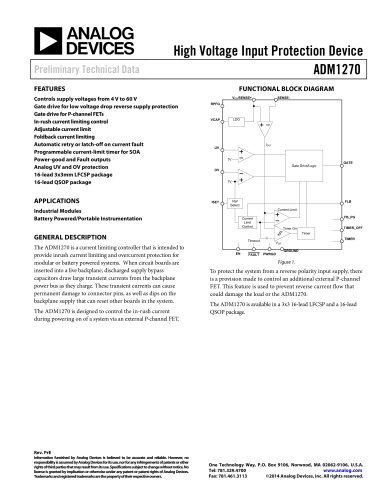
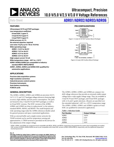
RFIN2
VGAIN1
VSW1
VSW1
VGAIN2
RFOUT2
RFIN3
VPOS1
VPOS2
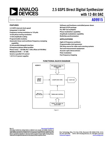
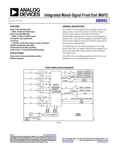
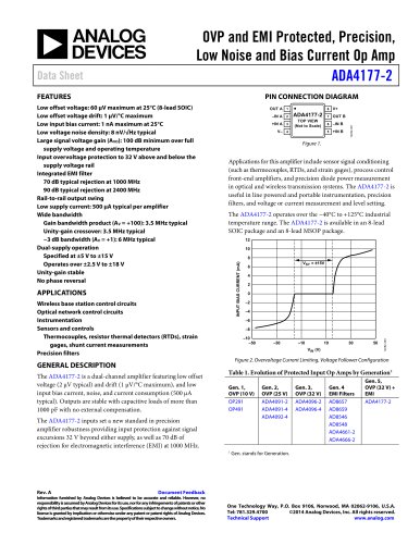
FUNCTIONAL BLOCK DIAGRAM
30
15
6
13
16
18
21
11
28
RFOUT1 32
AMP3
AMP1
VVA1
VVA2
2
ADL5246
AMP2
4
5
7
8
9
12 14 17 19 22
NIC
1
EP
3
10 20 23 24 25 27 29 31
GND
12233-001
RFIN1
26 RFOUT3
Figure 1.
Rev. 0
Document Feedback
Information furnished by Analog Devices is believed to be accurate and reliable. However, no
responsibility is assumed by Analog Devices for its use, nor for any infringements of patents or other
rights of third parties that may result from its use. Specifications subject to change without notice. No
license is granted by implication or otherwise under any patent or patent rights of Analog Devices.
Trademarks and registered trademarks are the property of their respective owners.
One Technology Way, P.O. Box 9106, Norwood, MA 02062-9106, U.S.A.
Tel: 781.329.4700
©2014 Analog Devices, Inc. All rights reserved.
Technical Support
www.analog.com