عضویت
عضویت  ورود اعضا
 راهنمای خرید


Very fast 900V/µs, 4A Power Amplifier0 pages
PA119CE • PA119CEA
PA119CE • PA119CEA
PA119CE, PA119CEA
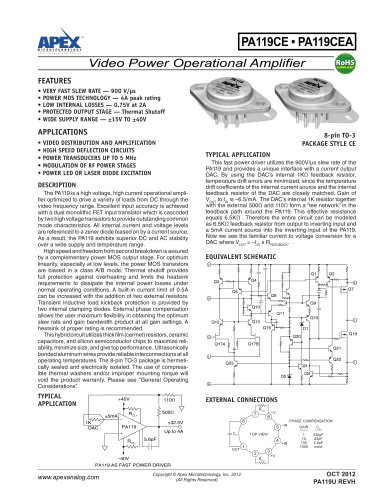
Video Power Operational Amplifier
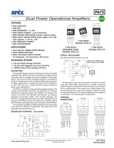
FEATURES
• VERY FAST SLEW RATE — 900 V/µs
• POWER MOS TECHNOLOGY — 4A peak rating
• LOW INTERNAL LOSSES — 0.75V at 2A
• PROTECTED OUTPUT STAGE — Thermal Shutoff
• WIDE SUPPLY RANGE — ±15V TO ±40V
APPLICATIONS
8-pin TO-3
PACKAGE STYLE CE
• VIDEO DISTRIBUTION AND AMPLIFICATION
• HIGH SPEED DEFLECTION CIRCUITS
• POWER TRANSDUCERS UP TO 5 MHz
• MODULATION OF RF POWER STAGES
• POWER LED OR LASER DIODE EXCITATION
TYPICAL APPLICATION
DESCRIPTION
The PA119 is a high voltage, high current operational amplifier optimized to drive a variety of loads from DC through the
video frequency range. Excellent input accuracy is achieved
with a dual monolithic FET input transistor which is cascoded
by two high voltage transistors to provide outstanding common
mode characteristics. All internal current and voltage levels
are referenced to a zener diode biased on by a current source.
As a result, the PA119 exhibits superior DC and AC stability
over a wide supply and temperature range.
High speed and freedom from second breakdown is assured
by a complementary power MOS output stage. For optimum
linearity, especially at low levels, the power MOS transistors
are biased in a class A/B mode. Thermal shutoff provides
full protection against overheating and limits the heatsink
requirements to dissipate the internal power losses under
normal operating conditions. A built-in current limit of 0.5A
can be increased with the addition of two external resistors.
Transient inductive load kickback protection is provided by
two internal clamping diodes. External phase compensation
allows the user maximum flexibility in obtaining the optimum
slew rate and gain bandwidth product at all gain settings. A
heatsink of proper rating is recommended.
This hybrid circuit utilizes thick film (cermet) resistors, ceramic
capacitors, and silicon semiconductor chips to maximize reliability, minimize size, and give top performance. Ultrasonically
bonded aluminum wires provide reliable interconnections at all
operating temperatures. The 8-pin TO-3 package is hermetically sealed and electrically isolated. The use of compressible thermal washers and/or improper mounting torque will
void the product warranty. Please see “General Operating
Considerations”
.
TYPICAL
APPLICATION
+40V
±5mA
1K
DAC
110Ω
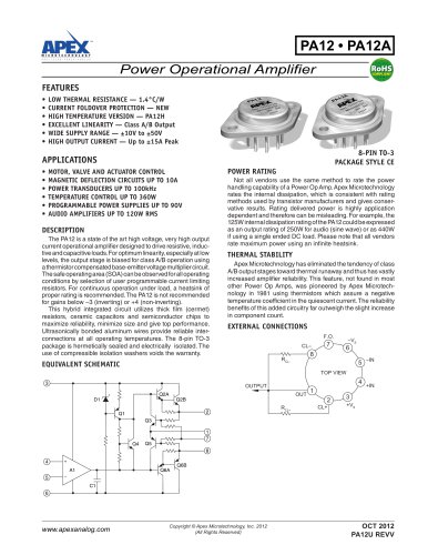
EQUIVALENT SCHEMATIC
3
Q1
Up to 4A
Q5
Q8
Q9
Q10
Q11
Q15
Q13
Q12
Q16
1
D1
Q19
Q20
5
Q17B
Q17A
Q21
4
Q22
Q23
Q24
D2
7
Q25
6
EXTERNAL CONNECTIONS
7
RCL-
6
8
CC
–V
5 –IN
TOP VIEW
5.6pF
4
OUT
–40V
PA119 AS FAST POWER DRIVER
www.apexanalog.com
PA119U
2
Q7
8
±32.5V
PA119
Q2
Q4
Q3
500Ω
RCL+
RCL–
This fast power driver utilizes the 900V/µs slew rate of the
PA119 and provides a unique interface with a current output
DAC. By using the DAC’s internal 1KΩ feedback resistor,
temperature drift errors are minimized, since the temperature
drift coefficients of the internal current source and the internal
feedback resistor of the DAC are closely matched. Gain of
VOUT to IIN is –6.5/mA. The DAC’s internal 1K resistor together
with the external 500Ω and 110Ω form a “tee network” in the
feedback path around the PA119. This effective resistance
equals 6.5KΩ . Therefore the entire circuit can be modeled
as 6.5KΩ feedback resistor from output to inverting input and
a 5mA current source into the inverting input of the PA119.
Now we see the familiar current to voltage conversion for a
DAC where VOUT = –IIN x RFEEDBACK.
Copyright © Apex Microtechnology, Inc. 2012
(All Rights Reserved)
1
2
3
RCL+
+IN
PHASE COMPENSATION
GAIN
CC
1
10
100
1000
330pF
22pF
2.2pF
none
+V
OCT 2012
1
PA119U REVH