عضویت
عضویت  ورود اعضا
 راهنمای خرید


Solutions for 2.5D and 3D Test Tessent Support for Testing 3D-ICs0 pages
Solutions for 2.5D and 3D Test
Tessent Support for Testing 3D-ICs
Silicon Test and Yield Analysis
D A T A S H E E T
FEATURES:
■■ Tessent 2.5D support included in
the TSMC Chip on Wafer on
Substrate (CoWoS™) Reference
Flow.
■■ Advanced contactless IO test
capabilities improve wafer-level
test quality necessary for KGD.
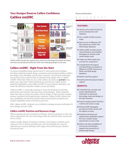
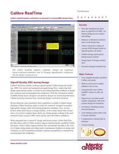
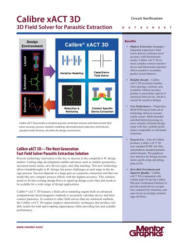
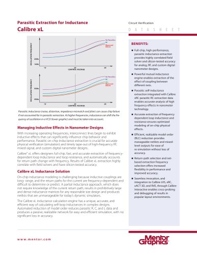
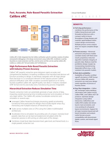
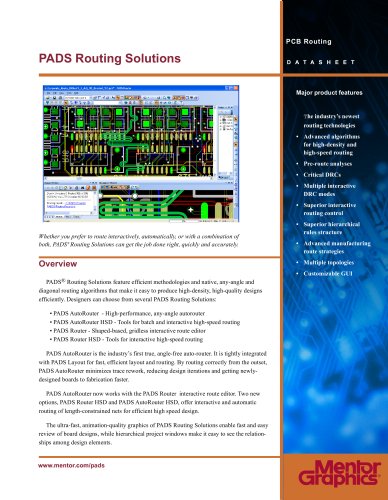
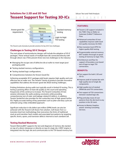
The Tessent suite of products provide solutions for key 3D IC test challenges.
Challenges in Testing 3D IC Designs
The next phase of semiconductor designs will include the adoption of 3D IC
packages. These vertical stacks of multiple bare die connected directly with
through-silicon vias (TSVs) present three new test challenges to the industry:
■■ Managing the escape rate of defective die at wafer to meet target postpackaging yield.
■■ Testing stacked memory configurations.
■■ Testing stacked logic configurations.
■■ Comprehensive Solutions for Known Good Die
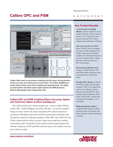
Achieving acceptable 3D IC package yield levels requires high-quality and costeffective test at wafer sort. The Tessent® family of products provide innovative
capabilities that address the known-good-die (KGD) testing challenges.
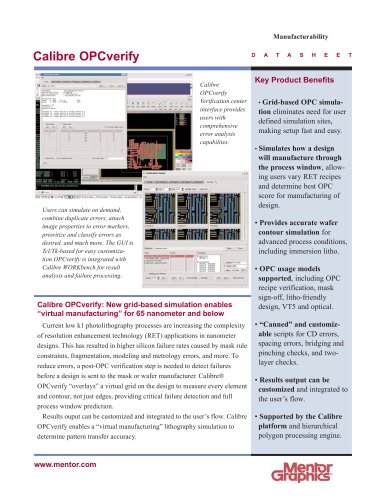
Probing limitations during wafer test typically result in limited IO testing. This is
having a growing effect on bare die quality as the count and operating
frequencies of IOs continue to increase. The Tessent Contactless IO test
solution eliminates the wafer probing constraints while providing
comprehensive test of static and leakage-related IO defects. In addition,
Tessent SerdesTest also provides for the contactless test of high-speed SerDes
IOs. Highly accurate testing of key parameters such as jitter and duty cycle are
achieved using a fully embedded approach.
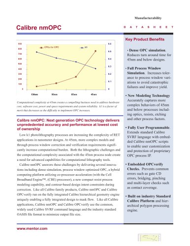
Significant reduction in die defect-per-million (DPM) levels can also be
achieved with the Tessent Cell-Aware Test solution. Cell-Aware Test is a
transistor-level test methodology that overcomes the limits of traditional
stuck-at and transition fault models and associated test patterns by targeting
specific shorts, opens, and transistor defects internal to each standard cell.
Testing Stacked Memories
Tessent MemoryBIST supports the test and diagnosis of memory die stacked
on top of a silicon interposer or directly on top of a logic die. A BIST engine is
integrated into the logic die and communicates to the TSV-based memory bus
w w w. m e nto r. co m /si li co n -y i e l d
■■ New transistor-level ATPG for
higher quality KGD testing.
■■ Programmable external memory
BIST enables thorough at-speed
testing of memory-to-logic TSVs.
■■ Architecture and flow for
support of boundary scan based
test of logic-to-logic TSV
connections.
BENEFITS:
■■ Test support for both 2.5D and
3D ICs
■■ Improve yield of stacked die with
high-quality test of single die
components.
■■ High-quality test of stacked
DRAM die and TSV connections.
■■ Test support of TSV connections
between stacked logic die.
■■ Plug-and-play reuse of scan
patterns from the die level to any
position in the 3D stack.
■■ Access to Mentor Graphics
award- winning Consulting
Services.