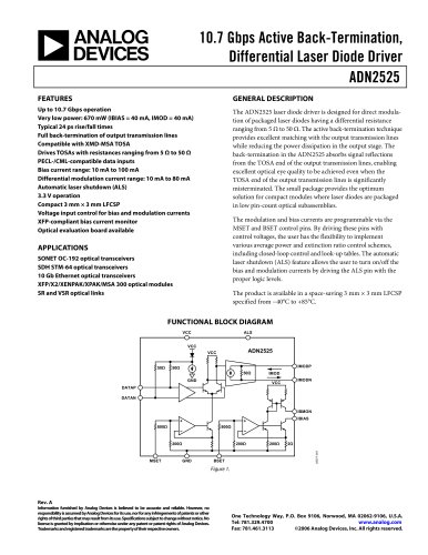
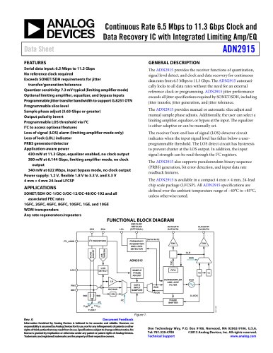
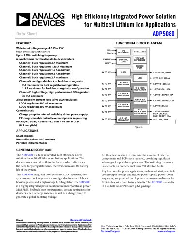
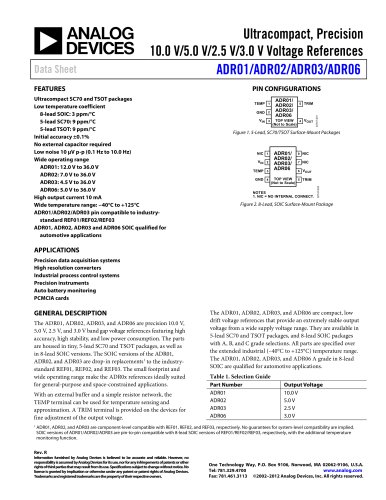
عضویت
عضویت  ورود اعضا
 راهنمای خرید


A 16-Bit, 6 MSPS SAR ADC System with Low Power Input Drivers and Reference Optimized for Multiplexed Applications0 pages
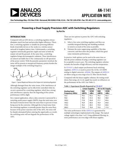
Circuit Note
CN-0307
Devices Connected/Referenced
AD7625
ADA4897-1/
ADA4897-2
Circuits from the Lab™ reference circuits are engineered and
tested for quick and easy system integration to help solve today’s
analog, mixed-signal, and RF design challenges. For more
information and/or support, visit www.analog.com/CN0307.
16-Bit, 6 MSPS, PulSAR, Differential ADC
Low Power, Low Noise, Single/Dual
Amplifier
Ultralow Noise XFET Voltage Reference
with Current Sink and Source Capability
2.7 V, 800 µA, 80 MHz Single/Dual Rail-toRail I/O Amplifier
ADR434
AD8031/
AD8032
A 16-Bit, 6 MSPS SAR ADC System with Low Power Input Drivers and Reference
Optimized for Multiplexed Applications
EVALUATION AND DESIGN SUPPORT
distortion [THD] = −110 dBc) at low power. The circuit is ideal
for high performance multiplexed data acquisition systems, such as
portable digital x-ray systems and security scanners, because the
SAR architecture can sample without the latency or pipeline delay
typically incurred with pipeline ADCs. The 6 MSPS sampling rate
allows fast sampling of multiple channels, and the ADC has true
16-bit dc linearity performance and a serial low voltage differential
signaling (LVDS) interface for low pin count and low digital noise.
Design and Integration Files
Schematics, Layout Files, Bill of Materials
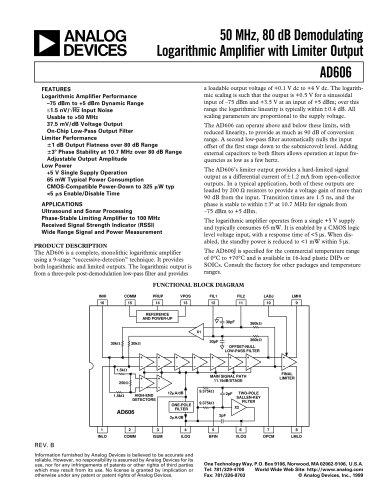
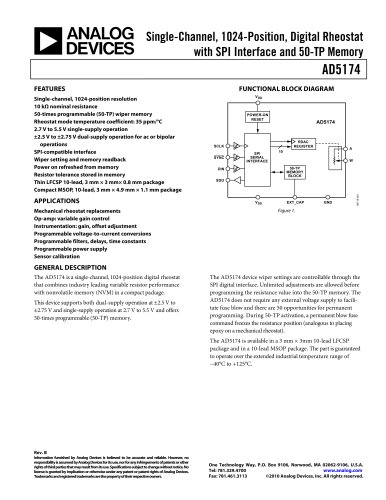
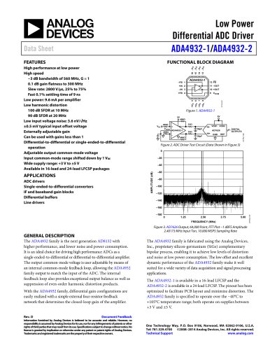
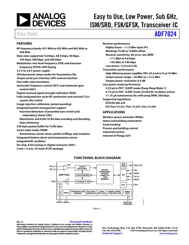
CIRCUIT FUNCTION AND BENEFITS
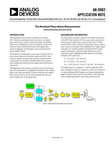
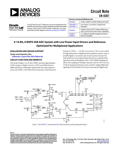
The circuit in Figure 1 is a 16-bit, 6 MSPS, successive approximation
(SAR) analog-to-digital converter (ADC) and differential-todifferential driver combination optimized for low noise (signal-tonoise ratio [SNR] = 88.6 dB) and low distortion (total harmonic
+5V
+4.096V
+7V
+4.096V
AD8031
ADR434
+5V
VDD +7V/+5V
0.1µF
VIN+
590Ω
20Ω
VCM
2.7nF
ADA4897-1
0.1µF
VREF = 4.096V
+2.5V
VCM = VREF ÷ 2
= 2.048V
49.9Ω
REFIN REF VDD1 VDD2 VIO
0.1µF
CNV+/
CNV–
100Ω
VIN+
VCM = 2.048V
IN+
–2V/0V VSS
VIN–
D+/D–
100Ω
DCO+/DCO–
100Ω
GND
AD7625
VDD +7V/+5V
0.1µF
VIN–
VCM = VREF ÷ 2
= 2.048V
49.9Ω
590Ω
0.1µF
VCM
IN–
20Ω
GND
2.7nF
ADA4897-1 0.1µF
VCM
CLK+/CLK–
100Ω
+2.048V
+5V
AD8031
11130-001
–2V/0V VSS
Figure 1. The ADA4897-1 Driving the AD7625 (All Connections and Decoupling Not Shown)
Rev. 0
Circuits from the Lab™ circuits from Analog Devices have been designed and built by Analog Devices
engineers. Standard engineering practices have been employed in the design and construction of
each circuit, and their function and performance have been tested and verified in a lab environment at
room temperature. However, you are solely responsible for testing the circuit and determining its
suitability and applicability for your use and application. Accordingly, in no event shall Analog Devices
be liable for direct, indirect, special, incidental, consequential or punitive damages due to any cause
whatsoever connected to the use of any Circuits from the Lab circuits. (Continued on last page)
One Technology Way, P.O. Box 9106, Norwood, MA 02062-9106, U.S.A.
Tel: 781.329.4700
www.analog.com
Fax: 781.461.3113
©2012 Analog Devices, Inc. All rights reserved.