عضویت
عضویت  ورود اعضا
 راهنمای خرید


PDC120M3B0 pages
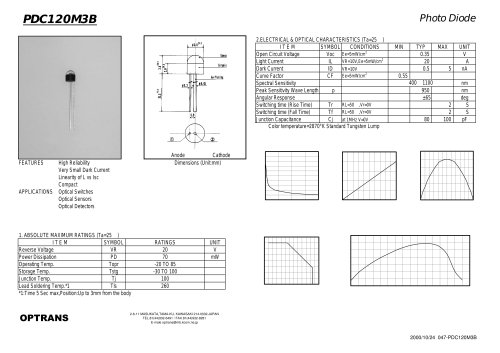
PDC120M3B
Photo Diode
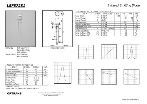
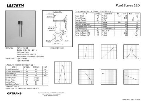
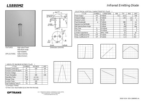
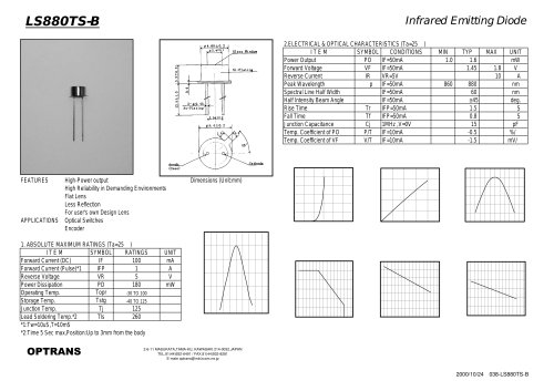
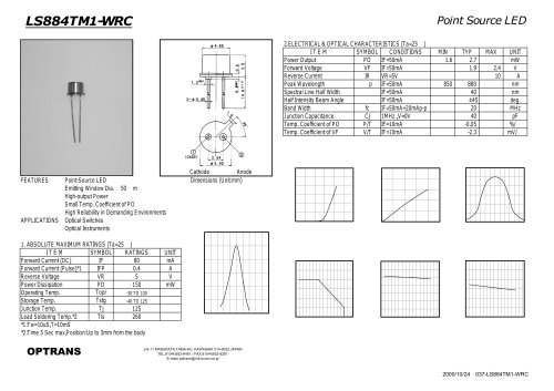
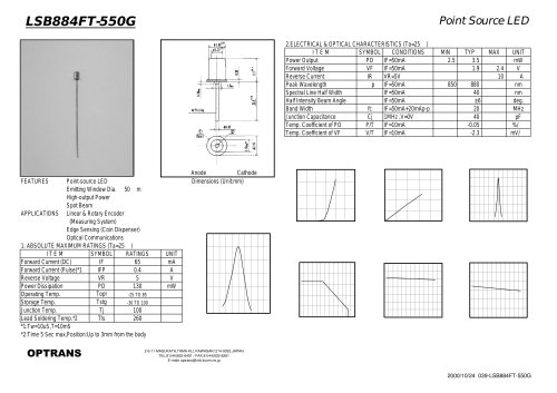
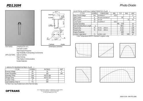
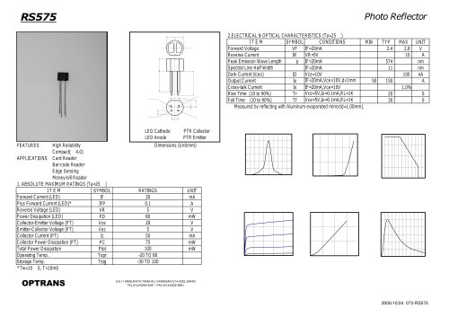
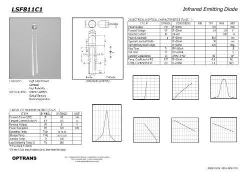
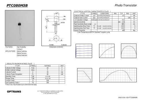
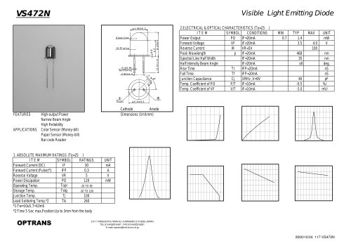
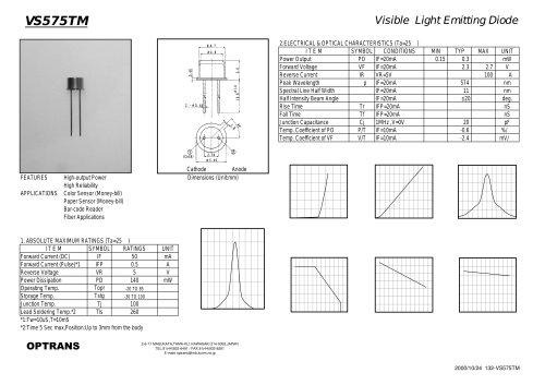
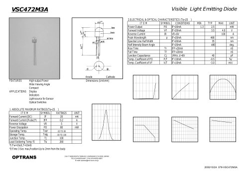
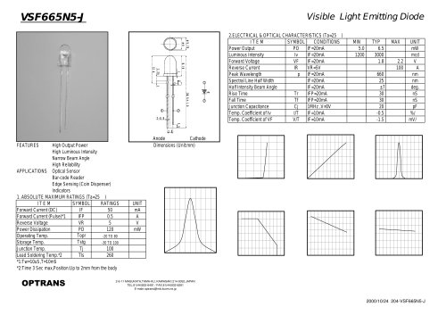
2.ELECTRICAL & OPTICAL CHARACTERISTICS (Ta=25 )
ITEM
CONDITIONS
SYMBOL
Open Circuit Voltage
Voc Ee=5mW/cm2
VR=10V,Ee=5mW/cm2
Light Current
IL
Dark Current
ID
VR=10V
Curve Factor
CF Ee=5mW/cm2
Spectral Sensitivity
p
Peak Sensitivity Wave Length
Angular Response
RL=50 ,Vr=0V
Switching time (Rise Time)
Tr
RL=50 ,Vr=0V
Switching time (Fall Time)
Tf
Junction Capacitance
Cj
at 1MHz V=0V
Color temperature=2870°K Standard Tungsten Lump
TYP
0.35
20
0.5
MAX
5
UNIT
V
A
nA
2
2
100
nm
nm
deg
S
S
pF
0.55
400
1100
950
±65
80
Anode
Cathode
Dimensions (Unit:mm)
High Reliability
Very Small Dark Current
Linearity of L vs Isc
Compact
APPLICATIONS Optical Switches
Optical Sensors
Optical Detectors
FEATURES
1. ABSOLUTE MAXIMUM RATINGS (Ta=25 )
ITEM
SYMBOL
Reverse Voltage
VR
Power Dissipation
PD
Operating Temp.
Topr
Storage Temp.
Tstg
Junction Temp.
Tj
Lead Soldering Temp.*1
Tls
*1:Time 5 Sec max,Position:Up to 3mm from the body
OPTRANS
MIN
RATINGS
20
70
-20 TO 85
-30 TO 100
100
260
UNIT
V
mW
2-6-11 MASUKATA,TAMA-KU, KAWASAKI 214-0032.JAPAN
TEL.81(44)932-6491 / FAX.81(44)932-8281
E-male optrans@mb.kcom.ne.jp
2000/10/24 047-PDC120M3B
"